LED中英文翻译,百度中英文翻译
本作品内容为LED中英文翻译,格式为 doc ,大小 80896 KB ,页数为 15页
('FirstLEDSummary一LED概述LED(LightEmittingDiode),light-emittingdiode,isasolidstatesemiconductordevices,whichcanbedirectlyconvertedintoelectricitytolight.LEDistheheartofasemiconductorchip,thechipisattachedtooneendofastent,isthenegativeside,theotherendofthepowerofthecathode,theentirechippackagetobeepoxyresin.Semiconductorchipiscomposedoftwoparts,partoftheP-typesemiconductor,itinsidethehole-dominated,theothersideistheN-typesemiconductor,hereismainlyelectronic.Butlinkingthetwosemiconductors,amongthemtheformationofa"PNjunction."Whenthecurrentthroughthewiresroleinthischip,willbepushinge-P,Pzoneintheholewithelectroniccomposite,andthentobeissuedintheformofphotonenergy,andthisistheprincipleofLEDluminescence.Thewavelengthoflightthatisthecoloroflight,isformedbythePNjunctionofthedecisionsofthematerial.LED(LightEmittingDiode),发光二极管,是一种固态的半导体器件,它可以直接把电转化为光。LED的心脏是一个半导体的晶片,晶片的一端附在一个支架上,一端是负极,另一端连接电源的正极,使整个晶片被环氧树脂封装起来。半导体晶片由两部分组成,一部分是P型半导体,在它里面空穴占主导地位,另一端是N型半导体,在这边主要是电子。但这两种半导体连接起来的时候,它们之间就形成一个“P-N结”。当电流通过导线作用于这个晶片的时候,电子就会被推向P区,在P区里电子跟空穴复合,然后就会以光子的形式发出能量,这就是LED发光的原理。而光的波长也就是光的颜色,是由形成P-N结的材料决定的。SecondLEDhistoryanddevelopment50yearsago,peoplehavetounderstandsemiconductormaterialscanproducelightofthebasicknowledge,thefirstcommercialdiodesin1960.EnglishistheLEDlightemittingdiode(LED)acronym,anditsbasicstructureisanelectroluminescentsemiconductormaterials,placedinawirerack,thensealedwithepoxyresinaround,thatis,solidpackage,Therefore,theprotectionoftheinternalbatteriescanplaytheroleofline,sotheseismicperformanceLEDgood.LEDisthecoreoftheP-typesemiconductorandcomponentsoftheN-typesemiconductorchips,theP-typesemiconductorandN-typesemiconductorbetweenatransitionlayer,calledthePNjunction.InsomesemiconductormaterialsinthePNjunction,theinjectionofasmallnumberofcarrier-carrierandthemajorityoftheextratimewillbeintheformoflightenergytorelease,thusthepowertodirectconversionofsolarenergy.PNjunctiononreversevoltage,afewhard-carrierinjection,itisnotluminous.Thisuseofinjectionelectroluminescentdiodesisproducedbytheprincipleoflight-emittingdiodes,commonlyknownasLED.Whenitinapositivestateofthework(thatis,atbothendswithforwardvoltage),thecurrentflowsfromtheLEDanode,cathode,semiconductorcrystalsontheissuefromtheultraviolettoinfraredlightofdifferentcolors,lightandthestrengthofthecurrents.InstrumentsusedforthefirstLEDlightsourceinstructions,butallkindsoflightcoloredLEDlightsintrafficandlargescreenhasbeenwidelyapplied,haveaverygoodeconomicandsocialbenefits.The12-inchredtrafficlightsasanexample,isusedintheUnitedStateshavelonglife,low-efficiency140wattincandescentword文档可自由复制编辑lampasalightsource,itproduced2,000lumensofwhitelight.Theredfilter,theloss-90percent,only200lumensofredlight.Inthelightofthenewdesign,Lumiledscompanieshave18redLEDlightsource,includingthelossofcircuit,atotalpowerconsumptionof14wattstogeneratethesameopticaleffect.AutomotiveLEDlightsisalsothesourceofimportantareas.Forgenerallighting,peopleneedmorewhitelightsources.The1998whiteLEDsuccessfuldevelopment.ThisistheGaNLEDchipandYttriumAluminumGarnet(YAG)packagetogethercause.GaNchipoftheBlu-ray(λp=465nm,Wd=30nm),madeofhigh-temperaturesinteringoftheCe3+YAGphosphorsexcitedbythisBlu-rayafterirradiatingayellow,thepeak550nm.Blue-chipinstalledintheLED-basedWanxingreflectioninthecavity,coveredwitharesinmixedwithYAGthinlayer,about200-500nm.LED-basedtabletsissuedbytheBlu-rayabsorptionpartofthephosphor,thephosphoranotherpartoftheBlu-rayandayellowlightmixed,canbeawhite.Now,theInGaN/YAGwhiteLED,YAGphosphorbychangingthechemicalcompositionofthephosphorlayerandadjustthethicknessofthe3500-10000Kcolortemperaturecanbecoloredwhite.ThisblueLEDthroughthemethodbywhite,constructedsimple,low-cost,hightechnologyismature,sousethemost.ThedevelopmentofLEDdisplaycanbedividedintothefollowingphases:firstphase1990to1995,mainlymonochromeand16colorgraphicsscreen.Usedtodisplaytextandsimpleimages,mainlyusedinrailwaystations,financialsecurities,banks,postofficesandotherpublicplaces,aspublicinformationdisplaytools.Thesecondstageisfrom1995to1999,therehavebeen64,256levelgray-scaletwo-colorvideoscreen.Videocontroltechnology,imageprocessing,opticalfibercommunicationtechnologyapplicationswillenhancetheLEDdisplaytoanewlevel.LEDdisplaycontrolLSIchipsspecialatthistimedevelopedbydomesticcompanies,andcanbeapplied.Thethirdstage,from1999,red,puregreen,blueLEDinbulkintoChina,whiledomesticenterprisesin-depthresearchanddevelopmentwork,usingred,green,andblueLEDproductionoffull-colordisplayhasbeenwidelyused,pouredintosportsstadiums,conventioncenters,squaresandotherpublicplaces,whichwillbringthedomesticlarge-screenfull-colorera.WiththerapiddevelopmentofLEDmaterialsmarket,surfacemountdeviceisavailablefrom2001,mainlyusedinindoorfullcolor,anditshighbrightness,colorful,lowtemperaturecharacteristics,thepointspacingcanbeadjustedbydifferentpriceRequirementswereaccepted,injusttwoyearstime,productsaleshavemorethan300millionyuan,surfacemountfull-colorLEDdisplayapplicationmarketenteredthenewcentury.Tomeetthe2008OlympicGames,"downsizing"plan,Liarddevelopedasurfacemountdualcolordisplays,alotoftimeforthetrainingcenterandgamescoring.FullcolorinOlympicvenues,inordertotighteninvestment,fullcolorwayismostlydetachable,liveduringtheOlympicGamesasatoolcanbeusedforrentalaftertheevent,astheperformanceofnationalpoliciessuchaspublicplaces,toolsreleasedbyInthiswaycostrecoveryassoonaspossible.Onthemarket,China\'saccessiontoWTO,Beijing\'ssuccessfulOlympicbidandsoon,intothedevelopmentofLEDdisplayindustry,anewopportunity.DomesticLEDdisplaymarketcontinuestogrow,currentlyinthedomesticmarket,domesticLEDdisplaymarketshareofnearly95%.LEDdisplaytheword文档可自由复制编辑internationalmarketcapacityisexpectedto30%ayeargrowthrate.Currently,LEDdisplaymanufacturersconcentratedprimarilyinJapan,NorthAmerica,ChinaLEDmanufacturersinwhichtheinsignificantshareofexports.Accordingtoincompletestatistics,theworld,thereareatleast150manufacturersfullcolor,inwhichproductsarecomplete,thelargercompanyhassome30orso.二LED历史及发展现状50年前人们已经了解半导体材料可产生光线的基本知识,第一个商用二极管产生于1960年。LED是英文lightemittingdiode(发光二极管)的缩写,它的基本结构是一块电致发光的半导体材料,置于一个有引线的架子上,然后四周用环氧树脂密封,即固体封装,所以能起到保护内部芯线的作用,所以LED的抗震性能好。发光二极管的核心部分是由P型半导体和N型半导体组成的晶片,在P型半导体和N型半导体之间有一个过渡层,称为P-N结。在某些半导体材料的PN结中,注入的少数载流子与多数载流子复合时会把多余的能量以光的形式释放出来,从而把电能直接转换为光能。PN结施加反向电压时,少数载流子难以注入,故不发光。这种利用注入式电致发光原理制作的二极管叫发光二极管,通称LED。当它处于正向工作状态时(即两端加上正向电压),电流从LED阳极流向阴极时,半导体晶体就发出从紫外到红外不同颜色的光线,光的强弱与电流有关。最初LED用作仪器仪表的指示光源,后来各种光色的LED在交通信号灯和大面积显示屏中得到了广泛应用,产生了很好的经济效益和社会效益。以12英寸的红色交通信号灯为例,在美国本来是采用长寿命、低光效的140瓦白炽灯作为光源,它产生2000流明的白光。经红色滤光片后,光损失90%,只剩下200流明的红光。而在新设计的灯中,Lumileds公司采用了18个红色LED光源,包括电路损失在内,共耗电14瓦,即可产生同样的光效。汽车信号灯也是LED光源应用的重要领域。对于一般照明而言,人们更需要白色的光源。1998年白光的LED开发成功。这种LED是将GaN芯片和钇铝石榴石(YAG)封装在一起做成。GaN芯片发蓝光(λp=465nm,Wd=30nm),高温烧结制成的含Ce3+的YAG荧光粉受此蓝光激发后发出黄色光射,峰值550nm。蓝光LED基片安装在碗形反射腔中,覆盖以混有YAG的树脂薄层,约200-500nm。LED基片发出的蓝光部分被荧光粉吸收,另一部分蓝光与荧光粉发出的黄光混合,可以得到得白光。现在,对于InGaN/YAG白色LED,通过改变YAG荧光粉的化学组成和调节荧光粉层的厚度,可以获得色温3500-10000K的各色白光。这种通过蓝光LED得到白光的方法,构造简单、成本低廉、技术成熟度高,因此运用最多。LED显示屏的发展可分为以下几个阶段:第一阶段为1990年到1995年,主要是单色和16级双色图文屏。用于显示文字和简单图片,主要用在车站、金融证券、银行、邮局等公共场所,作为公共信息显示工具。第二阶段是1995年到1999年,出现了64级、256级灰度的双基色视频屏。视频控制技术、图像处理技术、光纤通信技术等的应用将LED显示屏提升到了一个新的台阶。LED显示屏控制专用大规模集成电路芯片也在此时由国内企业开发出来并得以应用。第三阶段从1999年开始,红、纯绿、纯蓝LED管大量涌入中国,同时国内企业进行了深入的研发工作,使用红、绿、蓝三原色LED生产的全彩色显示屏被广word文档可自由复制编辑泛应用,大量进入体育场馆、会展中心、广场等公共场所,从而将国内的大屏幕带入全彩时代。随着LED原材料市场的迅猛发展,表面贴装器件从2001年面世,主要用在室内全彩屏,并且以其亮度高、色彩鲜艳、温度低的特性,可随意调整的点间距被不同价位需求者所接受,在短短两年多时间内,产品销售额已超过3亿元,表面贴装全彩色LED显示屏应用市场进入新世纪。为了适应2008年奥运会的“瘦身”计划,利亚德开发了表面贴装双基色显示屏,大量用于训练馆和比赛计时计分系统。在奥运场馆全彩屏方面,为紧缩投资,全彩屏大部分采用可拆卸方式,奥运期间可作为实况转播工具,赛事结束后可用于租赁,作为演出、国家政策发布等公共场合应用工具,通过这种方式可尽快收回成本。就市场而言,中国加入WTO、北京申奥成功等,成为LED显示屏产业发展的新契机。国内LED显示屏市场保持持续增长,目前在国内市场上,国产LED显示屏的市场占有率近95%。国际上LED显示屏的市场容量预计以每年30%的速度在增长。目前,LED显示屏的主要制造厂商集中在日本、北美等地,我国LED制造厂商出口的份额在其中微不足道。据不完全统计,世界上目前至少有150家厂商生产全彩屏,其中产品齐全,规模较大的公司约有30家左右。ThirdLEDadvantagesConductorlight-emittingdiode(LED)asathird-generationsemiconductorlightingsource.Thisfantasticproducthasalotofadvantages:(1)efficientlight:spectraofalmostallconcentratedinthevisiblelightfrequency,theefficiencycanreach80%-90%.Theluminousefficiencyofincandescentvisiblelightefficiencyofalmost10%-20%only.(2)highqualityoflight:notasaresultofspectrumUVandinfrared,thereisnoheat,noradiation,istypicallyagreenlightillumination.(3)energyconsumptionofthesmall:singlepowergenerally0.05-1w,throughtheclustercanbetailoredtomeetdifferentneeds,andwasteverylittle.Asalightsource,underthebrightnessinthesamepowerconsumptionofonlyordinaryincandescent1/8-10.(4)longlife:fluxattenuationto70%ofthestandardlifeexpectancyis100,000hours.Asemiconductorlightcanbeusedundernormalcircumstances50years,evenifthelonglifeofthepeople,lifewillbeuseduptotwolights.(5)durableandreliable:Notungstenwire,glassandothereasilydamagedcomponents,non-normalretirementrateisverysmall,verylowmaintenancecosts.(6)theapplicationofflexibility:smallsize,canflatpack,easytodevelopintoashortthinproducts,makepoint,line,facevariousformsofspecificapplications.(7)Security:workingvoltage1.5-5vorlessinbetweenthecurrent20-70mAinbetween.(8)green:recyclablewaste,nopollution,unlikefluorescentlampscontainingmercuryasingredients.(9)responsetimeisshort:toadapttofrequentandhigh-frequencyswitchingoperationofoccasions.三LED优点导体发光二极管(LED)作为第三代半导体照明光源。这种产品具有很多梦幻般优点:(1)光效率高:光谱几乎全部集中于可见光频率,效率可以达到80%-90%。而光效差不多的白炽灯可见光效率仅为10%-20%。(2)光线质量高:由于光谱中没有紫外线和红外线,故没有热量,没有辐射,属于典型的绿色照明光源。(3)能耗小:单体功率一般在0.05-1w,通过集群方式可以量体裁衣地满足不同word文档可自由复制编辑的需要,浪费很少。以其作为光源,在同样亮度下耗电量仅为普通白炽灯的1/8-10。(4)寿命长:光通量衰减到70%的标准寿命是10万小时。一个半导体灯正常情况下可以使用50年,即使长命百岁的人,一生最多也就用2只灯。(5)可靠耐用:没有钨丝、玻壳等容易损坏的部件,非正常报废率很小,维护费用极为低廉。(6)应用灵活:体积小,可以平面封装,易开发成轻薄短小的产品,做成点、线、面各种形式的具体应用产品。(7)安全:单位工作电压大致在1.5-5v之间,工作电流在20-70mA之间。(8)绿色环保:废弃物可回收,没有污染,不像荧光灯一样含有汞成分。(9)响应时间短:适应频繁开关以及高频运作的场合FourthClassificationofLEDdisplay1,colorbycolorcanbedividedintoSingle-colordisplay:Singlecolor(redorgreen).Two-colordisplay:redandgreendual-color,256grayscalelevels,candisplay65,536colors.Full-colorscreen:red,green,bluecolor,256grayscalefullcolordisplaycandisplaymorethan16millionkindsofcolors.2,accordingtodisplaydeviceclassificationLEDDigitalDisplay:7segmentdisplaydevicesforthedigitalcontrolcode,suitableforproductionoftheclockscreen,theinterestratescreens,showingthenumberofelectronicdisplay.LEDdot-matrixgraphicdisplay:displaydeviceisarrangedbyanumberofuniformcompositionofthedot-matrixLEDdisplaymodules,suitableforbroadcasttext,imageinformation.LEDvideodisplay:displaydevicesareformedbyanumberoflight-emittingdiodesthatcandisplayvideo,animationandothervideofiles.3,byusingtheoccasioncategoriesIndoorDisplay:LEDspotssmaller,generalΦ3mm-Φ8mm,showsthegeneralareaofafewtomorethantensquaremeters.OutdoorDisplay:dozensofsquaremetersinsizetoseveralhundredsquaremeters,highbrightness,canworkinthesun,withwind,rain,waterresistant.4,classifiedaccordingtolightspotdiameterIndoorscreen:Φ3mm,Φ3.75mm,Φ5mm,Roomexternalscreen:Φ10mm,Φ12mm,Φ16mm,Φ19mm,Φ20mm,Φ21mm,Φ22mm,Φ26mmRoomexternalscreenasthebasicunitoflightemittingtube,LEDtubeprincipleisasetofred,green,andbluelight-emittingdiodesealedinaplasticbarrelandjointlydevelop5,Displayastatic,horizontalscroll,verticalscrollandflipdisplay.Oneblockmodulecontroldrive12(uptocontrol24)8X8DotMatrix,atotalof16X48dotmatrix(or32X48dotmatrix),isasingleblockofMAX7219(orPS7219,HD7279,ZLG7289and8279,andthelikeLEDdisplaydrivermodule)12times(or24times)!Canuse"cascade"approachthecompositionofanylargedotmatrixdisplay.Effects,goodpowerconsumption,andtheMAX7219circuitthantheuseoflowercost.四LED显示屏的分类word文档可自由复制编辑1、按颜色基色可以分为单基色显示屏:单一颜色(红色或绿色)。双基色显示屏:红和绿双基色,256级灰度、可以显示65536种颜色。全彩色显示屏:红、绿、蓝三基色,256级灰度的全彩色显示屏可以显示一千六百多万种颜色。2、按显示器件分类LED数码显示屏:显示器件为7段码数码管,适于制作时钟屏、利率屏等,显示数字的电子显示屏。LED点阵图文显示屏:显示器件是由许多均匀排列的发光二极管组成的点阵显示模块,适于播放文字、图像信息。LED视频显示屏:显示器件是由许多发光二极管组成,可以显示视频、动画等各种视频文件。3、按使用场合分类室内显示屏:发光点较小,一般Φ3mm--Φ8mm,显示面积一般几至十几平方米。室外显示屏:面积一般几十平方米至几百平方米,亮度高,可在阳光下工作,具有防风、防雨、防水功能。4、按发光点直径分类室内屏:Φ3mm、Φ3.75mm、Φ5mm、室外屏:Φ10mm、Φ12mm、Φ16mm、Φ19mm、Φ20mm、Φ21mm、Φ22mm、Φ26mm室外屏发光的基本单元为发光筒,发光筒的原理是将一组红、绿、蓝发光二极管封在一个塑料筒内共同发5、显示方式有静态、横向滚动、垂直滚动和翻页显示等。单块模块控制驱动12块(最多可控制24块)8X8点阵,共16X48点阵(或32X48点阵),是单块MAX7219(或PS7219、HD7279、ZLG7289及8279等类似LED显示驱动模块)的12倍(或24倍)!可采用“级联”的方式组成任意点阵大显示屏。显示效果好,功耗小,且比采用MAX7219电路的成本更低。FifthLEDapplicationsItisasemiconductorlight-emittingdiodebycontrollingthedisplay,whichprobablylooklikethatfromlotsofsmallredlightsareusuallyformedbythebrightlightsofftoshowcharacter.Usedtodisplaytext,graphics,images,animations,quotes,video,videosignalsandotherinformationonthedisplayscreen.GraphicdisplayandLEDdisplayintothevideodisplaybytheLEDmatrixblocks.GraphicdisplayscanbesynchronizedwiththecomputerdisplayChinesecharacters,Englishtextandgraphics;videodisplayusingmicro-computercontrol,graphics,images,andMao,real-time,synchronization,clearmessagetothebroadcastofavarietyofinformationdissemination,butalsoshowstwodimensional,three-dimensionalanimation,video,TV,VCDprogramsandliveon.LEDdisplayshowsthescreenbrightlycolored,three-dimensionalsenseofstrong,static,suchaspainting,movingasthefilmiswidelyusedinfinance,tax,business,telecommunications,sports,advertising,industrialenterprises,transport,educationsystems,stations,docks,airports,shoppingmalls,hospitals,hotels,banks,securitiesmarkets,constructionmarket,auctionhouses,industrialenterprisesinmanagementandotherword文档可自由复制编辑publicplaces.LEDdisplaycanshowchangesinthenumbers,text,graphicsandvideo;notonlycanbeusedintheindoorenvironmentcanalsobeusedforoutdoorenvironment,withaprojector,TVwall,LCDscreencannotmatchadvantage.五LED应用范围LED是一种通过控制半导体发光二极管的显示方式,其大概的样子就是由很多个通常是红色的小灯组成,靠灯的亮灭来显示字符。用来显示文字、图形、图像、动画、行情、视频、录像信号等各种信息的显示屏幕。LED显示屏分为图文显示屏和视频显示屏,均由LED矩阵块组成。图文显示屏可与计算机同步显示汉字、英文文本和图形;视频显示屏采用微型计算机进行控制,图文、图像并茂,以实时、同步、清晰的信息传播方式播放各种信息,还可显示二维、三维动画、录像、电视、VCD节目以及现场实况。LED显示屏显示画面色彩鲜艳,立体感强,静如油画,动如电影,广泛应用于金融、税务、工商、邮电、体育、广告、厂矿企业、交通运输、教育系统、车站、码头、机场、商场、医院、宾馆、银行、证券市场、建筑市场、拍卖行、工业企业管理和其它公共场所。LED显示屏可以显示变化的数字、文字、图形图像;不仅可以用于室内环境还可以用于室外环境,具有投影仪、电视墙、液晶显示屏无法比拟的优点。SixthLEDscreentestmethodAlookatScreensize,appearance,smoothness,withthescreenconnectionandsoonSecondlookafterthedeadpixelscreenlightup,notinnotwithinthescopeof(ingeneralthescreenisbasicallygonenow)Colorconsistency,displaytextisnormal,displaypictures,playfullscreenfullcolortowhite,red,green,andblue.六LED显示屏检验方法一看屏体规格,外观,平整度,屏内的连线等二看屏点亮后坏点,在不在不范围之内,(一般来说现在的屏基本上没有了)色差一致性,显示文字是否正常,显示屏图片等,全彩的要全屏打白色,红,绿,蓝。HowLightEmittingDiodesWorkLightemittingdiodes,commonlycalledLEDs,arerealunsungheroesintheelectronicsworld.Theydodozensofdifferentjobsandarefoundinallkindsofdevices.Amongotherthings,theyformthenumbersondigitalclocks,transmitinformationfromremotecontrols,lightupwatchesandtellyouwhenyourappliancesareturnedon.Collectedtogether,theycanformimagesonajumbotelevisionscreenorilluminateatrafficlight.Basically,LEDsarejusttinylightbulbsthatfiteasilyintoanelectricalcircuit.Butunlikeordinaryincandescentbulbs,theydon\'tword文档可自由复制编辑haveafilamentthatwillburnout,andtheydon\'tgetespeciallyhot.Theyareilluminatedsolelybythemovementofelectronsinasemiconductormaterial,andtheylastjustaslongasastandardtransistor.Inthisarticle,we\'llexaminethesimpleprinciplesbehindtheseubiquitousblinkers,illuminatingsomecoolprinciplesofelectricityandlightintheprocess.WhatisaDiode?Adiodeisthesimplestsortofsemiconductordevice.Broadlyspeaking,asemiconductorisamaterialwithavaryingabilitytoconductelectricalcurrent.Mostsemiconductorsaremadeofapoorconductorthathashadimpurities(atomsofanothermaterial)addedtoit.Theprocessofaddingimpuritiesiscalleddoping.InthecaseofLEDs,theconductormaterialistypicallyaluminum-gallium-arsenide.Inpurealuminum-gallium-arsenide,alloftheatomsbondperfectlytotheirneighbors,leavingnofreeelectrons(negatively-chargedparticles)toconductelectriccurrent.Indopedmaterial,additionalatomschangethebalance,eitheraddingfreeelectronsorcreatingholeswhereelectronscango.Eitheroftheseadditionsmakethematerialmoreconductive.AsemiconductorwithextraelectronsiscalledN-typematerial,sinceithasextranegatively-chargedparticles.InN-typematerial,freeelectronsmovefromanegatively-chargedareatoapositivelychargedarea.AsemiconductorwithextraholesiscalledP-typematerial,sinceiteffectivelyhasextrapositively-chargedparticles.Electronscanjumpfromholetohole,movingfromanegatively-chargedareatoapositively-chargedarea.Asaresult,theholesthemselvesappeartomovefromapositively-chargedareatoanegatively-chargedarea.AdiodecomprisesasectionofN-typematerialbondedtoasectionofP-typematerial,withelectrodesoneachend.Thisarrangementconductselectricityinonlyonedirection.Whennovoltageisappliedtothediode,electronsfromtheN-typematerialfillholesfromtheP-typematerialalongthejunctionbetweenthelayers,formingadepletionzone.Inadepletionzone,thesemiconductormaterialisreturnedtoitsoriginalinsulatingstate--alloftheholesarefilled,sotherearenofreeelectronsoremptyspacesforelectrons,andchargecan\'tflow.Togetridofthedepletionzone,youhavetogetelectronsmovingfromtheN-typeareatotheP-typeareaandholesmovinginthereversedirection.Todothis,youconnecttheN-typesideofthediodetothenegativeendofacircuitandtheP-typesidetothepositiveend.ThefreeelectronsintheN-typematerialarerepelledbythenegativeelectrodeanddrawntothepositiveelectrode.TheholesintheP-typematerialmovetheotherway.Whenthevoltagedifferencebetweentheelectrodesishighenough,theelectronsintheword文档可自由复制编辑depletionzoneareboostedoutoftheirholesandbeginmovingfreelyagain.Asaresult,thedepletionzonedisappears.WhenthenegativeendofthecircuitishookeduptotheN-typelayerandthepositiveendishookeduptoP-typelayer,electronsandholesstartmoving.IftheP-typesideisconnectedtothenegativeendofthecircuitandtheN-typesideisconnectedtothepositiveend,currentwillnotflow.Nocurrentflowsacrossthejunctionbecausetheholesandtheelectronsareeachmovinginthewrongdirection.WhenthepositiveendofthecircuitishookeduptotheN-typelayerandthenegativeendishookeduptotheP-typelayer,thedepletionzonegetsbigger.Theinteractionbetweenelectronsandholeshasaninterestingeffect--itgenerateslight!Inthenextsection,we\'llfindoutexactlywhythisis.HowCanaDiodeProduceLight?Lightisaformofenergythatcanbereleasedbyanatom.Itismadeupofmanysmallparticle-likepacketsthathaveenergy.Theseparticles,calledphotons,arethemostbasicunitsoflight.Photonsarereleasedasaresultofmovingelectrons.Inanatom,electronsmoveinorbitalsaroundthenucleus.Electronsindifferentorbitalshavedifferentamountsofenergy.Generallyspeaking,electronswithgreaterenergymoveinorbitalsfartherawayfromthenucleus.Foranelectrontojumpfromalowerorbitaltoahigherorbital,somethinghastoboostitsenergylevel.Conversely,anelectronreleasesenergywhenitdropsfromahigherorbitaltoalowerone.Thisenergyisreleasedintheformofaphoton.Agreaterenergydropreleasesahigher-energyphoton,whichischaracterizedbyahigherfrequency.Aswesawinthelastsection,freeelectronsmovingacrossadiodecanfallintoemptyholesfromtheP-typelayer.Thisinvolvesadropfromtheconductionbandtoalowerorbital,sotheelectronsreleaseenergyintheformofphotons.Thishappensinanydiode,butyoucanonlyseethephotonswhenthediodeiscomposedofcertainmaterial.Theatomsinastandardsilicondiode,forexample,arearrangedinsuchawaythattheelectrondropsarelativelyshortdistance.Asaresult,thephoton\'sfrequencyissolowthatitisinvisibletothehumaneye--itisintheinfraredportionofthelightspectrum.Thisisn\'tnecessarilyabadthing,ofcourse:InfraredLEDsareidealforremotecontrols,amongotherthings.Visiblelight-emittingdiodes(VLEDs),suchastheonesthatlightupnumbersinadigitalclock,aremadeofmaterialscharacterizedbyawidergapbetweentheconductionbandandthelowerorbitals.Thesizeofthegapdeterminesthefrequencyofthephoton--inotherwords,itdeterminesthecolorofthelight.Whilealldiodesreleaselight,mostdon\'tdoitveryword文档可自由复制编辑effectively.Inanordinarydiode,thesemiconductormaterialitselfendsupalotofthelightenergy.LEDsarespeciallyconstructedtoreleasealargenumberofphotonsoutward.Additionally,theyarehousedinaplasticbulbthatconcentratesthelightinaparticulardirection.LEDshaveseveraladvantagesoverconventionalincandescentlamps.Foronething,theydon\'thaveafilamentthatwillburnout,sotheylastmuchlonger.Additionally,theirsmallplasticbulbmakesthemalotmoredurable.Theyalsofitmoreeasilyintomodernelectroniccircuits.Butthemainadvantageisefficiency.Inconventionalincandescentbulbs,thelight-productionprocessinvolvesgeneratingalotofheat.Thisiscompletelywastedenergy,unlessyou\'reusingthelampasaheater.LEDsgenerateverylittleheat,relativelyspeaking.Amuchhigherpercentageoftheelectricalpowerisgoingdirectlytogeneratinglight,whichcutsdownontheelectricitydemandsconsiderably.Upuntilrecently,LEDsweretooexpensivetouseformostlightingapplications.Thepriceofsemiconductordeviceshasplummetedoverthepastdecade,however,makingLEDsamorecost-effectivelightingoptionforawiderangeofsituations.Whiletheymaybemoreexpensivethanincandescentlightsupfront,theirlowercostinthelongruncanmakethemabetterbuy.Inthefuture,theywillplayanevenbiggerroleintheworldoftechnology.TRANSIENTVOLTAGESUPPRESSOR(TVS)DiodePRESENTATION•Highprotectiononsensitivemobileelectronicdevices•FollowstrictlytotheIEC61000-4-2ESDteststandard•UsingthebehaviorofdiodeP/NjunctiontoachieveESDprotectionWhatareTransientVoltages?•Thesearefaultswhichcausethevoltagetogooutsidenormallimitsforaperiodoftime.Transientvoltagesarecharacterizedbythreethings:VeryHighVoltage,OccurForAVeryShortPeriodoftime(innanoseconds)andHighOccurrence.Manytransientscausedamagetomicro-semiconductorchipsetsbydegradingtheirperformance.Thisdamageiscumulativeandeventuallyreachesapointwheresuddenandcompletefailureofthecomponentresults.Moreover,sometransientsarecapableofcausingimmediateequipmentfailures.Equipmentfailurescausedbytransientsarehardtodetectandareoftenincorrectlyblamedonother‘perceived’causes.Microsemiconductorchipsetsdamagedbytransientsoftenrequiresophisticatedinstrumenttoreplacethemwhichmakethemexpensivetorepair.Theonlycureistoclamptransientstoasafelevelwheretheprotectedloadcanwithstand.TVSdiode’sAdvantages•TVSDiodevs.ZenerDiodeComparedwiththetraditionalZenerdiode,TVSdiodehasalargerP/Ncrosssection.TVSdiodecomponentisconstructedanddesignedtoabsorblargeramountsofenergy,joules,withafasterword文档可自由复制编辑responsetimethanZenerdiode.Zenerdiodehasahigherclampingvoltageandheatdissipationisslower.•TVSDiodevs.MultilayerMetaloxideVaristor,MLVAmajordifferencebetweenTVSdiodeandMLVis,asMLVabsorbstransientenergy,itselectricalparameterssuchasLeakagecurrentandBreakdownvoltagetendtodriftawayfromtheiroriginalspecificationswhichexhibitsaninherentwearoutmechanismwithinthestructure.Becauseofitshighimpedance,itsclampingratiocanreachashighas3.ThereforeMLVismoresuitabletobeappliedonlesssensitivelineswhereitshighclampingvoltagecanbetolerated.•TVSDiodevs.CeramicCapacitorCeramiccapacitorisnotabletowithstandahightransientvoltage.A10kVtransientvoltagewilldestroyabout60%ofthecomponentoftheceramiccapacitorwhileTVSdiodeisabletowithstandupto15Kvtransientvoltage.CeramiccapacitorisalsonotabletodissipateheatefficientlylikewhatTVSdiodedoeswhentransientoccurs.•TVSDiodevs.GasDischargeTubes,GDTsTVSdiodelimitsvoltagespiketoacceptablelevelbyclampingwhileGDTlimitsvoltagespikebycrowbaraction.GDTconductswhenitsthresholdvoltageisexceededandthentriggertoanon-statevoltageofonlyafewvolts.AdrawbackofGDTprotectionisthatthetriggeronstatevoltageisbelowtheoperatingvoltageoftheprotectedload.Theprotectedloadwillbeshutdowntemporarily.LED是如何工作的通常被称为LED的发光二极管,是电子世界中真正的无名英雄。LED的功能多达几十种,被广泛的应用于各种装置之中。在其他应用场合,LED可以作为数字钟的数码显示、传送来自遥控装置的数据、手表的背光灯以及指示各种器械何时开启。归纳起来,LED可以在巨大的电视荧屏上形成各种图像或者点亮交通灯。从本质上讲,LED就是一些小灯泡,所以很适合用于电子线路中。但与普通白炽灯泡不同的是,LED没有能烧尽的灯丝,而且使用过程中也不会变得很热。它们仅仅依靠半导体材料的电子运动来发光照明,并且其寿命和标准晶体管的一样长。在这篇文章里,我们将一起来探究一下这些普遍存在的有色眼镜后面的简单原则,对于揭示该过程中电气光学方面的潜规则具有一定的启发。那么什么是二极管呢?二极管是最简单的一种半导体元件。一般来说,半导体是在电流传导方面特性不唯一的一种材料。多数半导体是由内含杂质(其他材料的原子)的导体word文档可自由复制编辑制成的。添加杂质的过程被称为掺杂。在LED中,传导材料通常选用铝—镓—砷化物(AIGaAs)。在纯净的铝—镓—砷化物中,所有的原子和相邻原子间都非常完美地结合在一起,没有能自由运动的电子(带负电的粒子)传导电流。在掺杂过的材料中,添加的原子改变了原有的平衡,产生了自由电子或空穴。增加的这两种粒子都能增强该材料的传导性。因为电子带负电,故有多余电子的半导体被称为N型半导体。在N型半导体中,自由电子从负电区域移向正电区域。因为空穴带正电,故有多余空穴的半导体被称为P型半导体。电子可以在两个空穴之间来回移动,从负电区域移向正电区域。这样,从表面上看空穴是从正电区域移向负电区域。二极管是由制作在同一硅片上的P型半导体和N型半导体所组成,电极在两端引出。这种制作工艺使得二极管具有单向导电性。二极管两端不加电压是N区的自由电子和P区的空穴在两层的结合处进行复合形成耗尽层。在耗尽层中,半导体材料还原为绝缘状态—所有的空穴都和电子发生复合,所以没有自由移动的电子或存有电子的空间,电荷便不再流动。要去除耗尽,就必须获得由N区移向P区的自由电子和向相反方向移动的空穴。要达到这个目的,可以把二极管N区一端和P区一端分别和电路的负极和正极相连接。N区的自由电子被负极所排斥并推向正极。P区的空穴沿另一路径移动。当电极之间的电位差足够大时,耗尽层的电子和空穴分离又开始自由移动。结果,耗尽层消失。如果电路的负极连到N区,正极连到P区,那么电子和空穴就开始移动。如果P区一端连到电路的负极,N区一端连到电路的正极,则电流将停止流动。因为空穴和电子都向相反的方向移动,所以没有电流穿过PN结。当电路的正极和负极分别连接到二极管的N区和P区时,耗尽层加宽。有趣的是,在电子和空穴相互作用的过程中产生了光!接下来,我们将讨论一下其中的奥妙。二极管是怎样发光的呢?光是原子释放能量的一种形式。光有许多像存有能量的包裹一样的小微粒组成。这些微粒被称为光子,是光的基本单元。光子由移动的电子所释放。在一个原子中,电子沿特定的轨迹绕原子核作圆周运动。处于不同轨道的电子所含能量有所不同。一般而言,具有较高能量的电子在离核较远的轨道中运行。如果一个电子从低轨道进入高轨道,则一定有外界因素促使其能级发生变化。相反,电子从高轨道跃迁到低轨道时会释放能量。这种能量是以光子的形式释放出来的。能级差越大,跃迁时释放的光子能量越高,即频率越高。正如前面一段提及的那样,穿越二极管的自由电子能进入P区的空穴。这相当于一个微粒从传送通道落入较低的轨道,所以电子以光子的形式释放能量。事实上,任何二极管都存在这种现象,但只有特殊材料制成的二极管才能发出可见光。比如,在一个标准硅二极管中的原子按某种方式方式排列起来,这种方式使得电子跃迁的距离相对较短。结果,光子的频率就很低以至于人眼无法看到,这种频率的光子处于光谱中的红外线区域。当然,这未必很糟糕:和其他元器件相比,红外LED是遥控装置的首选。用于数字钟的数码显示的能发出可见光的二极管是由一种特殊材料制成,其特点是传导通道和低轨道间的沟道较宽。沟道的尺寸决定了光子的频率—换句话说,它决定了光的颜色。虽然所有的二极管能发光,但大多数并非有效。对于一个普通的二极管,半导体材料自身会消耗许多光能。LED特殊的构造使其易于向外射放大量的光子。再者,它们被封装在塑胶球状物中使得光子集中到一个特定的方向。同传统的白炽灯相比,LED有以下几点优势。首先,LED内没有回烧尽的灯丝,所以其寿命要长得多。其次,小体塑胶球形封装使LED更耐用。对于传统的白炽灯而言,在其工作过程中会产生大量的热。这完全是一种能源浪费,除非你想用灯泡作发热器。相对而言LED产生的热量非常少。大部分电功率将直接用于发光,这在很大程度上降低了电力需求。以前,LED的成本较高以至于无法将其广泛地用于照明。但在过去的十年里,半导体元件的成本急剧下降,使得LED在许多情况之下的照明元件选择上很划算。虽然到现在为止,LED的造价仍比白炽灯的高,但从长远来看其应用前景非常广阔。在不久的将来,LED会word文档可自由复制编辑在技术领域里发挥更大的作用。瞬态电压抑制二极管介绍•有效保护高感应可携式设备•根据及通过IEC国际静电测试标淮•应用二极管P/N结面的特性来达到静电保护原理什么是瞬态电压?瞬态电压是交流电路上电流与电压的一种瞬时态的畸变。浪涌、谐波为主要的表现形式。瞬态电压最主要的特点有三个:超高压,瞬时态,高频次。超高压是指通常的瞬态电压尖峰,高出正常电路电压幅值的好几倍。瞬时态是指瞬态电压持续的时间非常之短,它可以在数亿分之一秒内完成迸发到消失的过程。高频次是指瞬态电压的活动十分频繁,可以说无时不有、无处不在。瞬态电压是会对微电子半导体芯片造成损坏的。虽然有些微电子半导体芯片受到瞬态电压侵袭后,它的性能没有明显的下降,但是多次累积的侵袭会给芯片器件造成内伤而形成隐患。瞬态电压对芯片器件造成的损伤难以与其它原因造成的损伤加以区别,从而不自觉地掩盖了失效的真正原因。由于微电子半导体芯片的精、细、结构,如要替换或修理需要使用高度精密仪器,是非常费财的。为一的有效方法就是把瞬态电压抑制在被保护元件能承受的安全水平。瞬态电压抑制二极管的优势•瞬态电压抑制二极管与齐纳二极管与传统的齐纳二极管相较,瞬态电压抑制二极管的P/N结面积更大。这一结构上的改进使瞬态电压抑制二极管具更强的高压承受力和更快的效率。相较之下齐纳二极管也有较高的抑制电压和较慢的散热速度。•瞬态电压抑制二极管与多层金属氧化物突波吸收器瞬态电压抑制二极管与多层金属氧化物突波吸收器最大的不同是多层金属氧化物突波吸收器的功能会在瞬态电压的冲击下衰退。当瞬态电压侵袭时,多层金属氧化物突波吸收器的相关参数如漏电电流值和中止电压值都会偏离原来的参数而变得不准确。还有多层金属氧化物突波吸收器有较高的阻抗所以它的抑制电压可达最初中止电压的3倍,这种特性只適合用于对电压不太感应的线路和元件的保护。•瞬态电压抑制二极管与陶瓷电容器陶瓷电容器这类元件对高压的承受力比较弱。如有10kV的瞬态电压冲击时,会对陶瓷电容器造成约60%的损坏,而瞬态电压抑制二极管能承受到15kV的瞬态电压。在瞬态电压侵袭时所产生的热量,陶瓷电容器也没有办法象瞬态电压抑制二极管那样很有效的把它散去。•瞬态电压抑制二极管与离子气体放电管瞬态电压抑制二极管是以抑制电压的方式来达到瞬态电压保护,而离子气体放电管是以铁橇动作的方式来达到瞬态电压保护。离子气体放电管的缺点是在启动后保持在非常低的电压壮态,电压低于负载的正常工作电压。在这种情形下,负载没有办法绩续工作,会暂时的word文档可自由复制编辑关闭。word文档可自由复制编辑word文档可自由复制编辑',)
提供LED中英文翻译,百度中英文翻译会员下载,编号:1700754998,格式为 docx,文件大小为15页,请使用软件:wps,office word 进行编辑,PPT模板中文字,图片,动画效果均可修改,PPT模板下载后图片无水印,更多精品PPT素材下载尽在某某PPT网。所有作品均是用户自行上传分享并拥有版权或使用权,仅供网友学习交流,未经上传用户书面授权,请勿作他用。若您的权利被侵害,请联系963098962@qq.com进行删除处理。

 下载
下载 下载
下载 下载
下载 下载
下载 下载
下载 下载
下载 下载
下载 下载
下载 下载
下载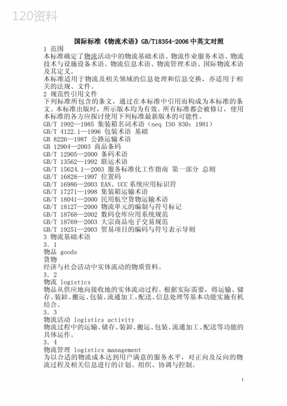 下载
下载 下载
下载 下载
下载